Ekaterine Chikoidze, Project coordinator, PhD
GEMaC, CNRS, UVSQ, Université Paris Saclay
ekaterine.chikoidze@uvsq.fr


The very concrete way to reach the target of Energy efficiency is to turn to more efficient power electronics. Increasing power density and power conversion optimization for CO2 emission reduction are key (Yole,Ltd). For Green Power Electronics and Energy saving advanced materials are one of the Key Enabling Technologies (KETs). Si-based device performances degrade badly at high temperatures, restricting their use for high power electronics. As an alternative there is a new generation of Wide Band Gap (WBG) semiconductors that have the capability to operate at higher temperatures, switching frequencies and voltages. This characteristic not only results in less losses but enables significantly reduced volume of power components due to decreased cooling requirements and smaller passive components, contributing to overall lower system cost. WBG integration into Energy application areas will result in energy savings estimated contribution into the ClimateAction (ReportORNL/TM-2017/702 ). Two major WBG materials with this potential which already made significant advances in power electronics are SiC and GaN, covering low and mid voltage (<3kV) range.
Exceeding them are the ultra wide band gap (UWBG) semiconductors (Eg>4eV), which should bring additional advantages with ability of sustaining very high voltages with low losses for switching, high temperature operation, necessary in application for grid, data centers and trains, electrical vehicles, aircrafts and ships. Among UWBG materials Ga2O3 has become a new challenger.

Versailles, France

Lyon, France

Paris, France

Barcelona, Spain

Swansea, UK

Orlanodo, USA

Tbilisi, Georgia

Raleigh, USA

GEMaC, CNRS, UVSQ, Université Paris Saclay
ekaterine.chikoidze@uvsq.fr

Institut des Nanosciences de Paris-INSP , Sorbonne Université
cantin@insp.jussieu.fr

Institut des Nanosciences de Paris-INSP , Sorbonne Université
zheng@insp.upmc.fr

GEMaC, CNRS, UVSQ, Université Paris Saclay
alain-soroush.abbasi-zargaleh@uvsq.fr

Institut des Nanosciences de Paris-INSP , Sorbonne Université
vonbarde@insp.jussieu.fr

Optical transmittance, reflectance, diffusion
&
Photoluminescence spectroscopy (PL)

The spinel group is a growing family of materials with general formulation AB2X4 (the X anion typically being a chalcogen like O and S) with many advanced applications for energy. At the time being, the spinel zinc gallate (ZnGa2O4) arguably is the ternary ultra-wide bandgap bipolar oxide semiconductor with the largest bandgap (~5eV), making this material very promising for implementations in deep UV optoelectronics and ultra-high power electronics. In this work, we further demonstrate that, exploiting the rich cation coordination possibilities of the spinel chemistry, the ZnGa2O4 intrinsic conductivity (and its polarity) can be controlled well over 10 orders of magnitude. p-type and n-type ZnGa2O4 epilayers can be grown by tuning the pressure, oxygen flow and cation precursors ratio during metal-organic chemical vapor deposition. A relatively deep acceptor level can be achieved by promoting antisites (ZnGa) defects, while up to a (n > 1019 cm-3) donor concentration is obtained due to the hybridization of the Zn-O orbitals in the samples grown in Zn-rich conditions. Electrical transport, atomic and optical spectroscopy reveal a free hole valence band conduction (at high temperature) for p-ZnGa2O4 while for n-ZnGa2O4 a (Mott) variable range hopping (VRH) and negative magnetoresistance phenomena take place, originated from “self-impurity” band located at Ev+ ~3.4 eV. Among arising ultra-wide bandgap semiconductors, spinel ZnGa2O4 exhibit unique self-doping capability thus extending its application at the very frontier of current energy optoelectronics.

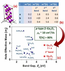
While there are several n-type transparent semiconductor oxides (TSO) for optoelectronic applications (e.g. LEDs, solar cells or display TFTs), their required p-type counterpart oxides are known to be more challenging. At this time, the n-type TSO with the largest bandgap (Eg=5 eV) is Ga2O3 that holds the promise of extending the light transparency further into the deep ultraviolet. In this work, it is demonstrated that strongly compensated Ga2O3 is also an intrinsic (or native) p-type TSO with the largest bandgap for any reported p-type TSO.
J. Mater. Chem. C, 2019, 7, 10231–10239 | 10235


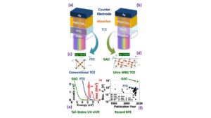
The use of ultra-wide bandgap transparent conducting beta gallium oxide (b-Ga2O3) thin films as electrodes in ferroelectric solar cells is reported. In a new material structure for energy applications, we report a solar cell structure (a light absorber sandwiched in between two electrodes – one of them -transparent) which is not constrained by the ShockleyeQueisser limit for open-circuit voltage (Voc) under typical indoor light. The solar blindness of the electrode enables a record-breaking bulk photovoltaic effect (BPE) with white light illumination (general use indoor light). This work opens up the perspective of ferroelectric photovoltaics which are not subject to the Shockley-Queisser limit by bringing into scene solar-blind conducting oxides.
https://doi.org/10.1016/j.mtener.2019.100350


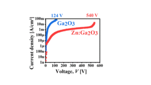
Which the actual critical electrical field of the ultra-wide bandgap semiconductor b-Ga2O3 is? Even that it is usual to find in the literature a given value for the critical field of wide and ultra-wide semi-conductors such as SiC (3 MV/cm), GaN (3.3 MV/cm), b-Ga2O3 (~8 MV/cm) and diamond (10 MV/cm), this value actually depends on intrinsic and extrinsic factors such as the bandgap energy, material residual impurities or introduced dopants. Indeed, it is well known from 1950’s that reducing the residual doping (NB) of the semiconductor layer increases the breakdown voltage capability of a semiconductor media(e.g. as N3=4 by using the Fulop’s approximation for an abrupt junction). A key limitation is, therefore,he residual donor/acceptor concentration generally found in these materials. We report that doping with amphoteric Zinc a p-type b-Ga2O3 thin films shortens free carrier mean free path (0.37 nm), resulting in the ultra-high critical electrical field of 13.2 MV/cm. Therefore, the critical breakdown field can be, at least, four times larger for the emerging Ga2O3 power semiconductor as compared to SiC and GaN. We further explain these wide-reaching experimental facts by using theoretical approaches based on the impact ionization microscopic theory and thermodynamic calculations.


11/07/2023, Versailles
Ultra-wide band gap semiconductors β-Ga2O3 and ZnGa2O4 electronic properties
Abstract:
In context of necessity of accelerating climate-saving actions by improving energy efficiency and reducing power consumption, ultra-wide band gap (Eg > 4.5 eV) β-Ga2O3 and ZnGa2O4 oxides are considered as promising materials for efficient power electronics devices. The objective of my PhD theses work was to investigate electronic properties of β-Ga2O3 and ZnGa2O4 thin films in order to disclose their real potentiality for applications in optoelectronics. By using multiple experimental characterization and analysis techniques for studding point defects the two problems were addressed: the realization/control of n-type and p-type conductivity and estimation/engineering critical electrical fields.

In this work we have demonstrated the first time that Zn doping of β-Ga2O3/r-sapphire thin film grown by MOCVD technique can exhibit a long-time stable room-temperature hole conductivity with a conductivity activation energy of around 86 meV. The origin of this level might be attributed then the donor-acceptor complex . (Figure) We believe that this study will add new evidences and will help to break a “taboo” related to the feasibility of room temperature hole conductivity in Ga2O3 via traditional growth technique and doping. We hope that we can inspire researchers to further study experimentally the point defects in β-Ga2O3.
(2024) -
- PDF download
(2024) -
- PDF download
(2024) -
- PDF download
(2024) -
- PDF download
(2023) -
- PDF download
(2023) -
- PDF download
(2022) -
- PDF download
(2022) -
- PDF download
(2022) -
- PDF download
(2022) -
- PDF download
(2021) -
- PDF download
(2021) -
- PDF download
(2021) -
(2020) -
- PDF download
(2020) -
- PDF download
(2020) -
- PDF download
(2019) -
- PDF download
(2019) -
- PDF download
(2019) -
- PDF download
(2018) -
- PDF download
(2017) -
- PDF download
(2016) -
- PDF download
We are continuously looking for motivated and talented students.
If you think that your CV could match the group activities, don’t hesitate to contact us.
Ultra-Wide Bandgap Semiconductors (UWBS) is an important class of materials that are used (or envisaged to be used) in a variety of applications, specifically related to the energy and electronics sectors. The present proposal, aims to establish the tradition for UWBS2E at Fall EMRS Meetings, serving as an arena for communicating the newest results in this booming field.
Scope:
Ultra-wide Bandgap Semiconductors (UWBS) exhibit unique properties for their applications in power electronics, RF electronics, deep UV optoelectronics, extreme-environment applications, etc. There is a range of material systems belonging to the UWBS class. In the present symposium, we keep our focus on oxides (e.g. Ga2O3, ZnGa2O4, ZnMgO, AlGa2O4, ect), nitrides (e.g. AlN, high-Al-content AlGaN, boron nitride, etc), even though contributions on other UWBS are welcome too. The goal is to cover full chain of topics: from material elaboration to device fabrication and performance, bringing together two sectors of the UWBS community: material researchers’ and device fabrication/simulation experts. We think that the UWBS community would enthusiastically meet our initiative to create an arena in this field so urgently needed in Europe. The EMRS symposium is an excellent format for this purpose, as we already learned from the success of the UWBS2E at 2022 and 2023Fall EMRS Meeting.

Visit Tbilisi state University in the framework of ERASMUS+ project.
Collaboration on Ga2O3.

wide-band-gap semiconductors
ultra wide-band-gap
energy
power electronics
optoelectronics
transparent electronics
deep UV
diodes
transistors
solar cells
photodetectors
LEDs
batteries
fuel cells

Ultra wide-band-gap semiconductors for energy and electronics (UWBG2E)


Contact :
Ekaterina Chikoidze
Ekaterine.chikoidze@uvsq.fr +33( 0)139255025
45 Ave Etats Unis
Versailles, France
78035